

PT2399 Tap Tempo
A Small Feature That Makes a Huge Impact

Overview
The PT2399 chip has been the go-to standard for DIY delays for years. It is a digital IC, but it is implemented much like any other analog component into various circuits. However, with all its advantages, it doesn't have an easy tap tempo function. There are a couple of commercially available solutions, such as the Taptation found at DIYstompboxes.com, but where's the fun in that? This is DIY, after all. This issue can all be remedied with the use of one of the many ubiquitous microcontrollers out there. In addition to being DIY and inexpensive, the project presented here has some great features, as well, including:
-
Relative time adjustments: Adjust your time relative to the tapped in tempo. Most solutions don't allow for this.
-
Time Division Switch: Easily configured switch for dividing the tempo. Default firmware allows for the original tapped in tempo as a quarter note as well as dotted eighth and eighth notes.
-
Easily modified: The code is all in Arduino, so it's easy to customize it for what you want it to do
-
Hardware Debouncing: Most solutions don't implement hardware switch debouncing, which helps make for more accurate tapped in tempo
-
Software Debouncing: Other solutions may include software debouncing, but the ones I have seen tend to use a debounce scheme that eats clock cycles and therefore limits how fast you can tap in.
In order to understand the hows and whys of this, let's talk a little bit about how the delay time is set on the PT2399. If you want even more detail, I highly recommend studying the fantastic PT2399 analysis at Electrosmash.
The delay time for the PT2399 is set by the amount of current that is sinked through pin 6. An internal +2.5V voltage is applied to pin 6, so the resistance placed from pin 6 to ground will determine how much current passes through it. This is achieved in most PT2399 delays with the use of a B50k potentiometer wired as a variable resistor and a small fixed resistor to prevent chip lockup. Note that as we increase the resistance, Ohm's law states that the current must be reduced because we have a constant voltage. As current decreases, delay time increases.
Implementations
Knowing that it is the amount of current sinked through pin 6 that sets delay time, we can then begin to think of approaches for how to have control over it. In reality, there are two approaches that are the most logical (get it?! a logic pun!). These will be discussed in detail below.
Digital Potentiometer
The approach used by the Taptation and advocated by many is the use of a microcontroller that controls a digital potentiometer. A digital potentiometer is an integrated circuit that has pins for the three standard pot lugs, power, ground, and serial communication. The serial communication is used to configure the internal arrays of resistors between the wiper and the two lugs. The advantage here is that it works very much like an analog potentiometer and it is relatively easy to work with.
Despite the functionality of this approach, there are some drawbacks that I personally don't like, including:
-
Tolerance: Digital potentiometers can have tolerances up to +/-20%, which can make precise determination of delay time difficult. This can require calibration or acceptance of the fact that there will be some variation.
-
Cost: Digital Potentiometers are another component and are typically even more expensive than the microcontroller used. It's not a huge deal, but some people are cost sensitive.
Pulse-Width Modulation
Another approach that can be used is to use the pulse-width modulation (PWM) output from the microcontroller. PWM is where an output pin of the microcontroller is switched between high and low (typically +5V and GND) very quickly. PWM is specified by the duty cycle (or percentage of time) that the signal is held high. A duty cycle of 100% is a constant 5V DC output. A 50% duty cycle will hold the output at +5V for an amount of time and then at GND for an equal amount of time.
The PWM output cannot be used directly, but with the use of a couple of common components, we can do some very clever things. In order to use the PWM, we need to do a few things:
-
Shift overall signal level from 0 to +5V to 0 to +2.5V to match pin 6 voltage level
-
Smooth signal so that it is continuous
-
Buffer signal
-
Apply signal to the base of a transistor that acts as a variable resistance from pin 6 to ground
-
Set a resistor to regulate current range and set a minimum delay time to prevent chip lockup
Below is a basic schematic showing how this is done. We will now discuss each of the steps and what each component in the schematic is doing.
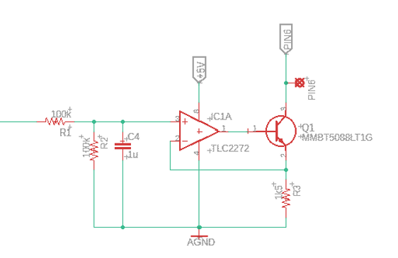
PWM Conversion Circuit
Voltage Division
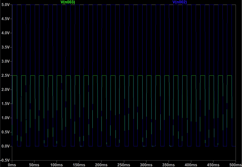
At the output of the PWM signal is a voltage divider. The equal value resistors result in a division of 1/2, which takes our 0 to +5V PWM signal and divides it to 0 to +2.5V, exactly as we need. The figure below shows the input and output of the voltage divider. It's pretty straightforward and exactly as you would expect.
Divided PWM Signal
Signal Smoothing
After the voltage divider, a large value capacitor is used to smooth the square PWM signal into a continuous DC signal. This will make it so that the current sinked through the transistor is consistent, resulting in a steady delay time. The output of the smoothing capacitor is shown below (the input is just the output of the previous plot). Note how it just looks like a steady DC voltage. The value of this voltage depends on the duty cycle. Note also that the value of the capacitor will have an effect on the amount of ripple as well as how long it takes the capacitor to charge. The plot below is showing steady state, but it took a couple seconds for the capacitor to fully charge after startup. The value of the capacitor needs to be chosen in conjunction with the PWM frequency. A very fast PWM signal requires less "smoothing" since it only needs to store enough charge to handle very short off periods in the PWM signal. A slow PWM signal requires a larger cap. For example, using the default PWM frequency of an ATTiny MCU of 490 Hz required a 47 uF cap, while a fast PWM frequency of 250 kHz was able to work easily with a 1 uF cap. The faster PWM frequency allows for a smaller cap and faster transition time between delay times, but comes at the cost of eating a little more power by running more frequently.

Smoothed PWM Signal
Signal Buffering
Once the signal is continuous, we want to buffer it to make sure that there is no loading one way or the other. This will also help in maintaining a consistent delay time. This is a unity gain buffer, so there is not really any point in showing the input versus output.
Pin 6 Gate
Now we take advantage of a really cool feature of transistors. When a voltage is applied to the base, the collector-to-emitter path starts to conduct. This is a function of the voltage on the base, so we feed our now smoothed and buffered voltage to the base of an NPN transistor. This will allow some amount of current to travel through the transistor to ground. The higher the duty cycle of the PWM, the more voltage we put on the transistor, which means we can sink more current and have a shorter delay time. If we have a low PWM, we conduct very little through the transistor and sink very little current, which results in longer delay times. Below are plots showing the current through the current resistor for 5, 50, and 90% duty cycles. Note how more current is sunk with the higher duty cycle. This means shorter delay time.

5% Duty Cycle Current Draw

50% Duty Cycle Current Draw
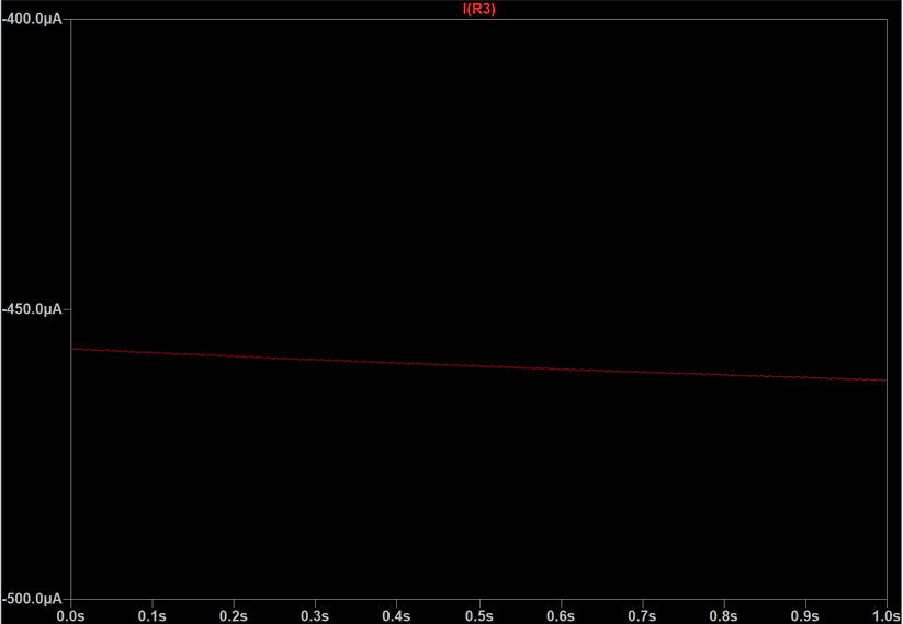
90% Duty Cycle Current Draw
Regulating Resistor
We want to make sure that we put a resistor from the transistor's collector to ground to ensure that we don't ever accidentally sink too much current. That can actually cause the chip to latch up and result in no delay signal, and it's just good practice. This resistor can also allow us to set the minimum and maximum amount of delay time. Making it larger means that we are reducing the maximum amount of current that can be sinked, raising the minimum delay time. Electrosmash gives a good analysis of this on his Time Manipulator project page, which is another fantastic resource and was the inspiration for this project.
The Project
Alright, we have talked a lot about the background here, so let's get to the project itself! Below you will find a schematic. In addition, you will need the following items (a full BOM is not provided, as the circuit is very straightforward and the schematic has everything labelled):
-
Arduino to act as programmer. Learn how to do that here. If you need to build a programmer, there are instructions right here.
-
ATTiny85 microcontroller
-
PT2399 delay circuit
-
Code (available on GitHub here)

PT2399 Tap Tempo Schematic
Hardware
With the schematic, let's break down the components of the project. We have:
-
Power section
-
ATTiny85
-
ATTiny ins/outs
-
PWM smoothing
The power section takes 5V in, which you will have for your PT2399 chip anyway. This should already be well regulated by your main delay circuit.
The ATTiny85 is shown with all of its pins. Some pin assignments can be changed to a degree, but if you are not very familiar with this style of microcontroller and don't want to spend a lot (and I mean a LOT) of time in the datasheet, just use what I used. For example, pin 1 is the reset pin and should never be pulled below 2.5V if you want the circuit to stay operational. Also, the PWM out should stay on pin 3. If you do make any changes, you MUST change them in the code. If you don't know which pins are which in the Arduino environment, this is a great reference.
You will notice that I have a handful of resistors and capacitors connected to the encoder and switches. These are low pass filters that serve as hardware debouncing of the switches. You see, when a mechanical switch gets thrown, there can be "bouncing" of the contacts, where the connection is literally made and broken multiple times as it settles to its new state. This can cause unexpected performance of the circuit. The hardware filters smooth these bounces out some, so that less debouncing has to be done in software, which is time consuming.
Finally, we see the PWM smoothing/current sink circuit at the top of the schematic. This is exactly what we looked at before. You will notice on the ATTiny85 version that there is one opamp that is unused. This is because we are only controlling a single chip. There is an ATTiny841 version (SMD only) that has outputs for two PT2399's so that you can do a stereo delay. Note that in this case, both outputs are identical. If you want to do divisions or something exotic like that, you can, but you will need to make the appropriate changes to the schematic, board layout, and code.
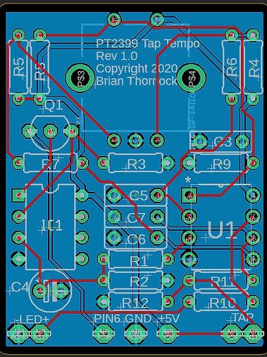
I made layouts from the above schematic and one adapted to the ATTiny841. They are available on my GitHub. Below is what they look like. The ATTiny85 through hole version measures 1.3"Wx2.25" high, while both SMD versions measure 0.85"x1.1", which is about the size of a 16mm potentiometer. The SMD boards are very densely populated, so if you have never done SMD before, I recommend some practice first.

PT2399 ATTiny85 SMD Layout

PT2399 ATTiny841 SMD Layout
PT2399 Through Hole Tap Tempo Board Layout
Software
Now let's look at the software somewhat. The code is heavily commented, and explains much of what is going on. However, we can think of it in terms of a couple of primary blocks, including:
-
Updating the multiplier
-
Monitoring the tap tempo switch
-
Updating the desired delay time
-
Updating the LED
-
Updating the PWM output
Updating the multiplier looks at the multiplier/division switch. If the switch is high (pressed) then it waits for a few milliseconds and checks again. If it is still high, it indicates that the multiplier has changed and sets a flag to be used later.
The tap tempo switch is not checked every cycle. Rather, it is driven by an interrupt so that we aren't wasting clock cycles looking to see if it was pressed. If it is pressed, a flag is set in the interrupt routine and then the normal processing cycle checks to see if that press is real. If it is real, it saves the time that the press happened and listens for more presses. Once we have at least 3 presses, it starts calculating the average time between taps. It will listen for up to 10 taps.
If either the multiplier, the tapped time, or the encoder changes, the desired delay time will be updated. This then gets passed to the LED and PWM updates, where the LED blinking rate and timing changes and the PWM duty cycle gets changed to match the desired delay time according to the conversion table.
While all of this is running, there are also pin change interrupts (PCI's) on the encoder pins. Because encoder pulses are short, we want to start listening to them right away. Whenever one of the two encoder pins changes voltage level, the microcontroller stops what it is doing and addresses the interrupt, then resumes normal operation. There is some brute force debouncing of the encoder in the interrupt, which is technically bad form, but it gives a much more consistent performance.
Basically, the software just does this over and over, the entire time it's powered on.
Summary
So there we have it: a PT2399 tap tempo controller that includes some great features, is easy to build, and will make your delay much more functional. There are lots of technical details out there, but I just wanted to make something that can get you going. Have fun with it, and if you do use this or reference it, I would appreciate a link and a mention. Thanks!